Samsung Foundry is stretching its advanced chip roadmap with more 2nm-class process options before moving into the 1.4nm era, a sign that the race for AI silicon is becoming less about one dramatic node jump and more about steady improvements in power, performance, memory density and design compatibility.
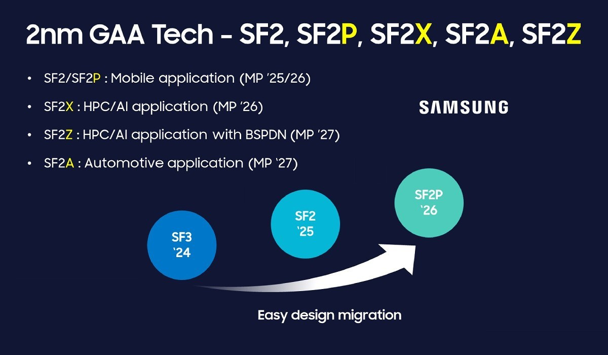
The company’s next major foundry story now sits around a wider 2nm family. Reports from Samsung’s foundry ecosystem discussions indicate that the roadmap will move from SF2 and SF2P into a performance-enhanced SF2P+ process before advancing to SF2X, a node aimed at artificial intelligence and high-performance computing customers. SF2P+ is reportedly targeted for mass production between 2027 and 2028, while SF2X will follow as a more specialized option for AI and HPC workloads.
That matters because the most advanced chip market is no longer driven only by smartphone processors. AI accelerators, data-center CPUs, custom inference chips and high-bandwidth memory systems are becoming the real battleground. Customers want better performance, but they also want stable design platforms, reusable IP and predictable manufacturing costs.
Samsung’s 2nm Roadmap Becomes the Bridge to 1.4nm
Samsung’s 1.4nm-class process, known as SF1.4, is now reportedly scheduled for mass production in 2029, with an enhanced SF1.4+ node expected in 2030. That is later than the company’s earlier long-term target, but it also reflects the reality of modern chip manufacturing: every generation is becoming harder, more expensive and more dependent on design-technology co-optimization.
Instead of rushing directly from 2nm to 1.4nm, Samsung appears to be building a longer transition through improved 2nm variants. That gives customers more options while giving the foundry more time to improve yield, packaging, power delivery and SRAM scaling.
One reported improvement is significant. Samsung’s move from SF2 to SF2P is said to reduce power consumption by 26% while raising operating frequency by 15%, with more than half of those gains coming from design-technology co-optimization, often shortened to DTCO.
In simple terms, DTCO means the chip design and manufacturing process are tuned together rather than treated as separate stages. At advanced nodes, that cooperation matters because shrinking transistors alone is no longer enough.
Why SRAM Is Becoming a Bigger Problem
One of the most important parts of Samsung’s roadmap is not only the transistor node itself, but how much SRAM can be packed onto chips.
SRAM is the fast memory used inside processors for registers and cache. It is much quicker than DRAM, but it also takes up more space. A typical SRAM bit cell uses six transistors, while a basic DRAM cell uses one transistor and one capacitor. That difference becomes critical as AI chips demand more on-chip memory for fast data movement.
This is why SRAM density has become a major issue for AI hardware. Modern accelerators do not only need raw compute. They need to move data quickly and repeatedly without wasting too much power. If data must constantly travel between the chip and external memory, performance suffers and energy use rises.
The shift can already be seen in AI accelerator design. Samsung Foundry has worked with AI chip companies such as Groq and Rebellions on advanced AI silicon, including projects using Samsung’s 4nm process. Rebellions previously said its next-generation Rebel AI chip would be produced on Samsung’s 4nm process and use Samsung HBM3E memory, while Samsung has also described collaboration with Arm, ADTechnology and Rebellions around AI chiplet platforms using Samsung’s 2nm GAA process and advanced packaging.
The Groq example shows why SRAM is now such a strategic topic. Reports around the Groq 3 LPU describe an inference-focused chip using 500MB of on-chip SRAM and extremely high memory bandwidth, showing how AI inference designs are moving toward specialized memory architectures rather than relying only on conventional GPU-style memory systems.
AI Is Changing What Foundry Customers Want
For years, foundry competition was often framed around who could reach the next node first. That still matters, but the AI era is changing the question. Customers now want process nodes that can support huge chips, chiplets, advanced packaging, fast memory, power efficiency and reliable yields.
That is why Samsung’s expanded 2nm roadmap is important. SF2P+ and SF2X are not just marketing labels. They are part of a longer effort to serve AI and HPC customers that may need different trade-offs from smartphone chipmakers. Some customers may prioritize frequency. Others may prioritize power efficiency, SRAM capacity, packaging, or compatibility with existing IP.
The same pattern is visible across the wider foundry industry. TSMC is also expanding its own 2nm-class portfolio, with N2P, N2X and N2U variants expected to serve different market needs over the next several years.
What 2nm and 1.4nm Actually Mean
It is also important to understand that terms such as 2nm and 1.4nm do not mean that every transistor feature is literally two nanometers or 1.4 nanometers wide. In today’s semiconductor industry, node names are best understood as generation labels. They describe a new class of technology that should offer better density, speed and power efficiency than the previous generation.
That does not make the labels meaningless. A better node can still deliver real advantages. But the gains now come from a combination of transistor architecture, power delivery, interconnect improvements, packaging, design tools, SRAM optimization and manufacturing yield — not only from shrinking one physical dimension.
The Bigger Picture for Samsung Foundry
Samsung’s challenge is execution. The company has strong technology assets, including gate-all-around transistor experience, memory leadership, advanced packaging and deep relationships in AI silicon. But in the foundry business, roadmaps are only as valuable as the yields and customer wins that follow.
The decision to build a broader 2nm bridge before SF1.4 suggests Samsung is trying to make its advanced foundry platform more practical for real customers. AI chipmakers need performance, but they also need manufacturable designs, predictable costs and enough flexibility to keep improving products without starting from zero every generation.
The 1.4nm era may still be several years away, but the battle for it is already being shaped now. Samsung’s immediate task is to prove that its 2nm family can become a strong foundation for AI chips, data-center processors and next-generation custom silicon.
If it succeeds, the road to 1.4nm will not be remembered as a delay. It will be seen as a carefully built bridge from today’s AI boom to the next decade of semiconductor manufacturing.


