Huawei has unveiled ambitious plans to develop semiconductor technology equivalent to 1.4nm chips by 2031 while introducing a new chip scaling framework that could challenge the long-standing dominance of Moore’s Law.
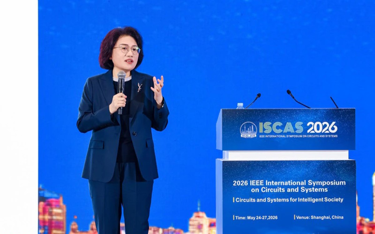
During a keynote presentation at the International Symposium on Circuits and Systems in Shanghai, Huawei revealed several major semiconductor advancements developed over the past six years, including a new architecture known as LogicFolding and a new chip development framework called the Tau Scaling Law.
The company argues that the semiconductor industry is reaching the practical and economic limits of traditional transistor shrinking methods, making alternative scaling approaches increasingly necessary.
Huawei Proposes Alternative to Moore’s Law
For more than five decades, Moore’s Law has guided semiconductor development by predicting that transistor density on integrated circuits would roughly double every two years.
The principle became the foundation for:
- Faster processors
- Smaller chips
- Lower power consumption
- Advancing computing performance
However, semiconductor manufacturers have increasingly struggled with:
- Physical transistor limitations
- Rising production costs
- Thermal constraints
- Slower efficiency gains
Huawei now believes the industry requires a fundamentally different scaling approach.
What Is Huawei’s Tau Scaling Law?
Huawei introduced what it calls the Tau Scaling Law, a new chip development model focused primarily on time-based performance optimization rather than purely geometric transistor shrinking.
Unlike Moore’s Law, which emphasizes smaller transistor dimensions, the Tau model reportedly focuses on:
- Signal propagation delay reduction
- Timing optimization
- System-level efficiency
- Architecture redesign
- Performance density improvements
Huawei argues that future semiconductor progress may depend more on:
- Intelligent architecture
- Data flow optimization
- Integrated system design
rather than simply reducing transistor size.
The company said it has already mass-produced 381 chips based on the Tau Scaling framework across multiple industries.
Huawei Unveils LogicFolding Architecture
Alongside the new scaling law, Huawei also introduced a new semiconductor architecture called:
- LogicFolding
According to the company, LogicFolding continuously compresses signal propagation delays while increasing transistor density efficiency.
Huawei says the architecture can be applied across:
- Semiconductor chips
- Circuit systems
- AI processors
- Integrated systems
- Future computing architectures
The company claims this approach could significantly improve computing efficiency without relying entirely on conventional node shrinking.
Read Also: Oppo Find N7 to Compete with iPhone Fold in 2026
Huawei Kirin Chips Will Adopt LogicFolding in 2026
Huawei confirmed that next-generation Huawei Kirin processors scheduled for release in 2026 will become the first commercial products using LogicFolding architecture.
The chips are expected to power future Huawei smartphones and may deliver:
- Improved AI processing
- Better energy efficiency
- Faster computing performance
- Enhanced multitasking capabilities
The first products using the architecture are expected to reach the market later this year.
Huawei’s growing investment in self-developed chip technology has become increasingly important as the company continues navigating restrictions linked to US sanctions and semiconductor supply limitations.
Huawei Targets 1.4nm-Equivalent Chips by 2031
One of the most attention-grabbing announcements involved Huawei’s long-term chip roadmap.
The company stated that by 2031 it expects to produce chips with transistor density equivalent to:
- 1.4nm process technology
While Huawei did not confirm it would literally manufacture chips using a traditional 1.4nm fabrication node, it suggested LogicFolding and Tau Scaling could achieve comparable transistor density and performance levels.
This distinction matters because modern semiconductor naming conventions increasingly function more as marketing labels than exact physical transistor measurements.
Semiconductor Industry Faces Physical Limits
Huawei’s announcement reflects a broader industry reality:
traditional semiconductor scaling is becoming increasingly difficult.
Modern chipmakers such as:
- Taiwan Semiconductor Manufacturing Company
- Samsung
- Intel
are all confronting escalating challenges involving:
- Quantum effects
- Heat dissipation
- Manufacturing complexity
- Rising capital costs
Advanced node production now requires:
- EUV lithography
- Massive infrastructure investment
- Highly specialized manufacturing tools
As a result, researchers increasingly explore alternative approaches beyond traditional transistor shrinking.
Huawei Pushes for Semiconductor Independence
The company’s aggressive semiconductor strategy also reflects China’s broader push toward technological self-sufficiency.
US export restrictions have limited Huawei’s access to:
- Advanced chips
- Manufacturing tools
- Semiconductor equipment
- Certain AI technologies
In response, Huawei has significantly expanded investment into:
- Domestic chip design
- Semiconductor R&D
- AI hardware
- System-level optimization
The company is now positioning itself not only as a smartphone maker but also as a major long-term semiconductor innovator.
AI Boom Increasing Semiconductor Pressure
The rapid growth of artificial intelligence is also accelerating demand for new semiconductor architectures.
AI workloads require:
- Massive parallel computing
- Faster data movement
- Lower latency
- Higher energy efficiency
Traditional chip scaling alone may no longer be sufficient to meet future AI computing requirements.
Architectural innovation — including approaches like LogicFolding — could therefore become increasingly important in the next phase of semiconductor development.
Collaboration Becoming Essential in Chip Industry
During the keynote, Huawei emphasized that semiconductor evolution can no longer rely on isolated company efforts.
The company called for:
- Global collaboration
- Industry openness
- Shared innovation
- Cross-sector partnerships
Huawei stated that no single company is likely capable of independently solving all technical barriers facing future semiconductor advancement.
This message comes as global semiconductor competition intensifies between:
- China
- United States
- Taiwan
- South Korea
- Europe
Why This Matters for Smartphones
If Huawei successfully commercializes LogicFolding and Tau Scaling technologies, future smartphones could benefit from:
- Faster AI processing
- Longer battery life
- Improved thermal efficiency
- More advanced photography
- Enhanced on-device computing
Huawei’s future Huawei Kirin processors may therefore become significantly more competitive against chips from:
- Qualcomm
- Apple
- MediaTek
particularly as AI-powered mobile computing becomes increasingly important.
Skepticism Likely to Remain
Despite the ambitious roadmap, industry analysts are likely to approach Huawei’s claims cautiously.
Achieving 1.4nm-equivalent density by 2031 would represent an enormous technological leap requiring:
- Advanced manufacturing breakthroughs
- Major materials innovation
- Sophisticated software optimization
- Supply chain expansion
The semiconductor industry has historically faced significant challenges when projecting long-term roadmap timelines.
Nevertheless, Huawei’s announcement signals that the global race for next-generation computing architectures is accelerating rapidly.
Frequently Asked Questions
What is Huawei’s Tau Scaling Law?
The Tau Scaling Law is Huawei’s proposed alternative to Moore’s Law focused on timing and system-level optimization.
What is LogicFolding?
LogicFolding is Huawei’s new semiconductor architecture designed to reduce signal delays and improve transistor density efficiency.
When will Huawei use LogicFolding chips?
Huawei says next-generation Huawei Kirin processors launching in 2026 will adopt the architecture.
What does 1.4nm-equivalent mean?
Huawei claims its future chips could achieve transistor density comparable to 1.4nm process technology by 2031.
Why is Moore’s Law becoming difficult?
Physical transistor limits, rising manufacturing costs, and thermal challenges are slowing traditional semiconductor scaling.
Conclusion
Huawei’s unveiling of the Tau Scaling Law and LogicFolding architecture marks one of the company’s most ambitious semiconductor announcements to date.
As traditional transistor scaling approaches the practical limits of Moore’s Law, Huawei is betting that architectural innovation and timing-based optimization could define the future of computing performance.
Whether the company can realistically achieve 1.4nm-equivalent chip density by 2031 remains uncertain, but the announcement highlights the rapidly intensifying global race to shape the next generation of semiconductor technology.


